POWER CONVERSION / 14 MIN READ
Capacitive DC-DC converters: how a charge pump works.
See how a charge pump doubles or inverts a voltage with switches and capacitors, why its output sags under load, and simulate both circuits in Simvolta.
By Simvolta · Updated
WATCH THE EXPLANATION · 6:17
How Does 5V Become 10V? | Charge Pump Explained
See how capacitors and switches turn a 5 V supply into nearly 10 V, and how switching frequency and load affect a charge-pump voltage doubler in Simvolta.
Playing loads YouTube’s privacy-enhanced player and connects to Google. You can read the guide without loading it.
English captions are automatically generated by YouTube. The written explanation below includes the circuit, equations and measured results.
Read the illustrated explanation ↓One supply, but you need a different voltage.
Your circuit runs from 5 V, but one part of it needs 10 V. Another wants −5 V. Classic examples are the ±10 V an RS-232 line driver needs from a 5 V logic supply, the bias for an LCD, or the higher voltage a flash memory uses while it writes. Converting one DC voltage into another is called DC-DC conversion.
Most people meet DC-DC conversion through inductor-based buck and boost converters. There is a simpler family that uses no inductor at all: capacitive converters, also called charge pumps or switched-capacitor converters. A few switches and capacitors, a clock, and the right sequence produce a doubled or inverted voltage.
This guide builds both a voltage doubler and a voltage inverter in Simvolta. Every result below is either calculated, and labelled as a prediction, or measured in the desktop solver, and labelled as a result.
A capacitor is a bucket of charge you can carry.
A capacitor stores charge Q in proportion to the voltage across it: Q = C · V. Charge it to 5 V, disconnect it, and it keeps those 5 V between its plates, wherever you move it. That is the whole trick. A charge pump fills a capacitor from the supply in one phase, then reconnects it somewhere else in the next phase.
The capacitor that moves is the flying capacitor, C1. If its negative plate is moved from ground to the 5 V supply, its positive plate rises to 5 V + 5 V = 10 V. Nothing in C1 changed; its reference point did. A second capacitor, the output or reservoir capacitor C2, collects these transfers and keeps the output steady between them.
Use the buttons to switch phases. The highlighted path is where conventional current flows in that phase; the voltages are the ideal, unloaded values.
Q = C · VE = ½ · C · V²
Phase 1, clock high: S1 and S2 close. Current flows from the 5 V supply through S1 into C1's top plate and out of its bottom plate through S2 to ground, charging C1 to 5 V. C2 alone supplies the load.
The voltage doubled; the energy did not. Each coulomb that reaches the output passes through the 5 V supply twice: once while it charges C1, once while C1 is stacked on top of the supply. The supply therefore delivers twice the output current, and input power is at least the output power. A charge pump changes voltage and current in opposite directions, just like a transformer or a boost converter.
Four switches, two capacitors and one clock.
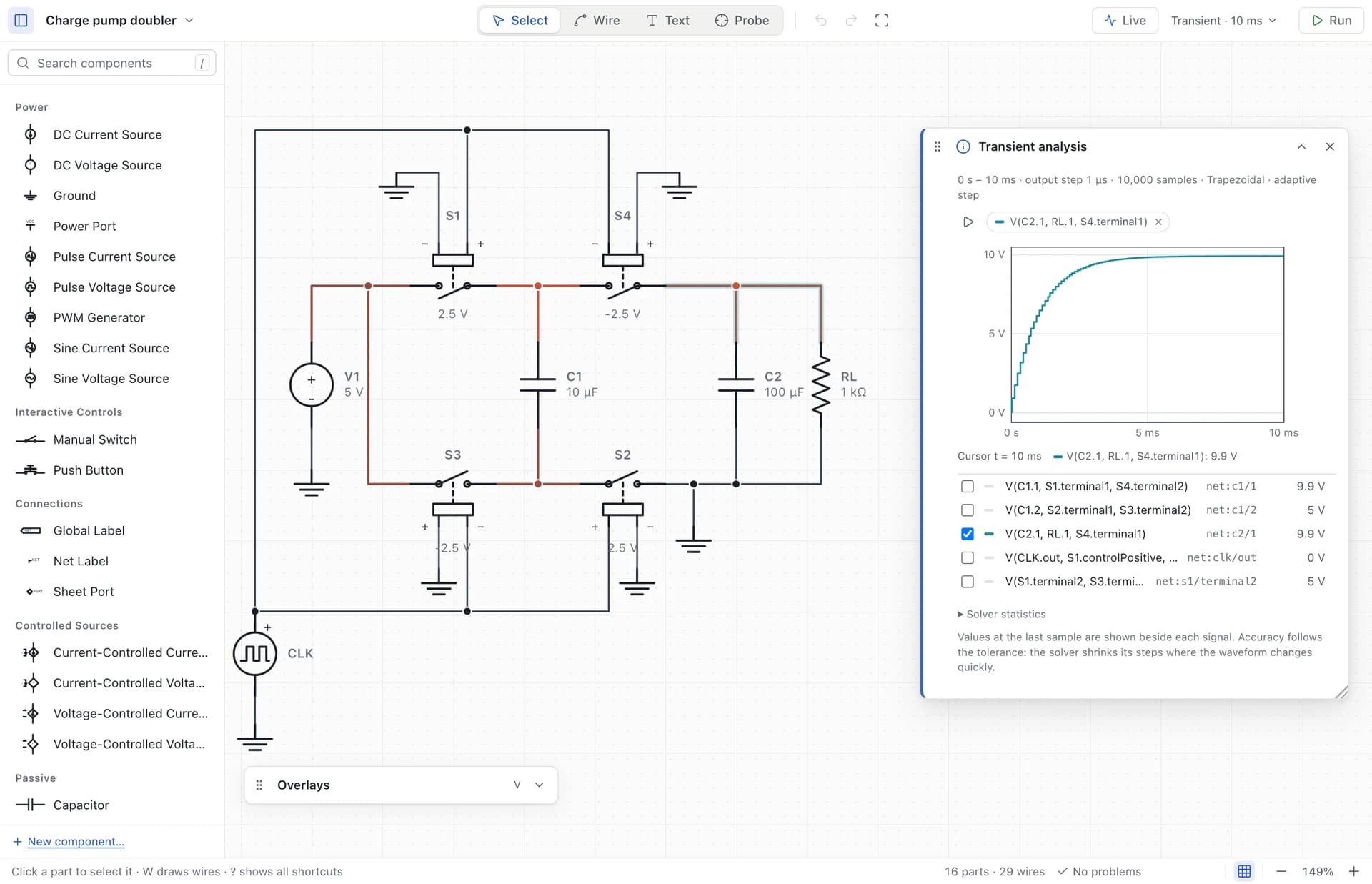
The doubler in the bundled example uses Simvolta's voltage-controlled switches as ideal electronic switches, the job MOSFETs do inside a charge-pump chip. A PWM generator is the clock: 0 V or 5 V, 10 kHz, 50 % duty.
S1 and S2 close while the clock is high: that is phase 1, which charges C1 across the supply. S3 and S4 close while the clock is low: phase 2, which stacks C1 on top of the supply and connects it to the output. To make S3 and S4 work in the opposite phase from the same clock, their control inputs are wired the other way round, clock to Ctrl− and ground to Ctrl+, and their threshold is set to −2.5 V. When the clock is low, their control voltage is 0 V, which is above −2.5 V, so they close.
| Part | Value | Role |
|---|---|---|
| V1 | 5 V DC | The only supply |
| CLK | 0 / 5 V, 10 kHz, 50 % | Sets the two phases |
| S1, S2 | threshold +2.5 V, 10 mΩ on | Phase 1: C1 across the supply |
| S3, S4 | threshold −2.5 V, 10 mΩ on | Phase 2: C1 on top of the supply, into the output |
| C1 | 10 µF | Flying capacitor: carries the charge |
| C2 | 100 µF | Output capacitor: holds VOUT between transfers |
| RL | 1 kΩ | The load |
Ground is the 0 V reference for every voltage in this guide. The example's switches use a 1 MΩ off resistance instead of the 100 MΩ default; that changes the output by less than 0.1 mV and keeps very fine output steps solvable (see Limits).
Step by step: charge, then stack.
Phase 1, clock high. S1 connects C1's top plate to 5 V and S2 connects its bottom plate to ground. C1 charges to 5 V. Meanwhile C2 is disconnected from C1 and alone supplies the load, so the output droops slightly.
Phase 2, clock low. S3 lifts C1's bottom plate to 5 V. C1 still holds about 5 V, so its top plate sits near 10 V, and S4 connects it to the output. C1 tops up C2 and supplies the load. The clock then goes high again and the cycle repeats 10,000 times a second.
The plot below is real solver output from the example, two clock periods after it has settled. Watch C1's plates move together: the bottom plate jumps between 0 V and 5 V, and the top plate follows it from 5 V to about 9.9 V, so the voltage across C1 hardly changes.
- C1 top plate
- C1 bottom plate
- VOUT
Predict the output before you run it.
With no load, C1 and C2 eventually charge to exactly 10 V and the converter stops moving charge. With a load, every coulomb the load takes must first be carried by C1, and that costs voltage. In the slow-switching limit, where each phase is long enough for the switch currents to finish, the charge pump behaves like an ideal 2 × source in series with a resistance of 1/(f · C1). Here that is 1 / (10 kHz × 10 µF) = 10 Ω.
So the predicted output is 10 V × 1 kΩ / (1 kΩ + 10 Ω) ≈ 9.90 V, the load current about 9.9 mA and the input current twice that: about 19.8 mA. The efficiency of this ideal-switch circuit is then VOUT / (2 × VIN) ≈ 99 %. The ripple estimate comes from the droop of C2 alone in phase 1, plus C2 and C1 together in phase 2.
R_out ≈ 1 / (f · C1) = 1 / (10 kHz × 10 µF) = 10 ΩVOUT ≈ 2 · VIN · RL / (RL + R_out) = 10 V × 1000 / 1010 ≈ 9.90 VI_in = 2 · I_out η = VOUT / (2 · VIN) ≈ 0.99ΔV ≈ I_out · (T / 2) · [1 / C2 + 1 / (C1 + C2)] ≈ 9.45 mV
- The switches are ideal apart from 10 mΩ on and 1 MΩ off: no gate charge, dead time or switching loss.
- Each phase lasts 50 µs, more than 250 times the time constant of the switches and capacitors (about 0.2 µs), so every transfer finishes: the slow-switching limit applies.
- The output is close to constant (C2 ≫ C1), and the result is read after start-up has finished.
Build it in Simvolta.
The video shows the whole build in the real desktop app, from an empty canvas to the result. Or open the finished circuit: choose Open Example… and pick Charge Pump Voltage Doubler.
Read the transcript
- Start with a 5 V supply.
- Add four voltage-controlled switches.
- C1 moves charge, C2 holds it, R1 is the load.
- Add a 10 kHz PWM clock and grounds.
- Press W, then wire the power path.
- Wire the clock to every switch.
- S3, S4: threshold −2.5 V, the other phase.
- Type C1 = 10u and C2 = 100u.
- Run a 10 ms transient.
- Probe VOUT: 5 V in, 9.9 V out.
- Change one thing: C1 = 1u.
- Run 100 ms: slower, and lower: ≈ 9.1 V.
- Place a DC voltage source (5 V is the default) and a ground. Add four voltage-controlled switches, two capacitors, a resistor and a PWM generator (its defaults are 0–5 V, 10 kHz, 50 %).
- Wire the power path: the source to S1 and S3; S1, C1's top plate and S4 together; S3, C1's bottom plate and S2 together; S4 to C2 and the load; S2, C2 and the load to ground.
- Wire the clock to Ctrl+ of S1 and S2 and to Ctrl− of S3 and S4. Connect each switch's other control pin to ground. Press W for the Wire tool; clicking empty canvas adds a bend, and ending on a wire makes a junction.
- Select S3 and S4 and set Threshold to -2.5. Set C1 to 10u and C2 to 100u. Keep the load at 1k.
- Choose Transient, 10 ms with a 1 µs output step, and press Run. Press P and click the load's wire to plot VOUT.
Run it: what the simulation shows.
The output climbs in small stairs. Each step is one phase-2 transfer: the first one shares C1's charge with an empty C2, and every later one closes about a tenth of the remaining gap, because C1 is a tenth of C2. That gives a start-up time constant of roughly eleven clock periods, about 1.1 ms. After 1 ms the output is at 6.12 V, after 5 ms at 9.82 V, and it then settles at 9.90 V.
- VOUT, C1 = 10 µF
- VOUT, C1 = 1 µF
- Predicted 9.90 V
- Predicted 9.09 V
| Quantity | Predicted | Simvolta | ngspice cross-check |
|---|---|---|---|
| VOUT, settled | 9.901 V | 9.900 V | 9.901 V |
| Ripple, peak to peak | 9.45 mV | 9.47 mV | 9.34 mV |
| Load current | 9.90 mA | 9.90 mA | – |
| Input current | 2 × I_out = 19.8 mA | 19.98 mA (from C1’s charge per cycle) | 19.6 mA (integrated) |
| Efficiency | 99.0 % | 99.0 % | – |
| VOUT at 1 ms / 5 ms | – | 6.12 V / 9.82 V | 6.12 V / 9.82 V |
Simvolta: transient 10 ms, 1 µs output step, adaptive trapezoidal integration; averages over the last millisecond, ripple over the last two clock periods. ngspice 47 ran the same netlist independently. The input current is not averaged from the plotted samples, because the switch current pulses last only a fraction of a microsecond and fall between 1 µs samples.
The predicted and simulated outputs differ by about 1 mV. The slow-switching formula ignores the 20 mΩ of the two closed switches and the small ripple, which accounts for the difference. The input current shows the energy bookkeeping: about 20 mA from 5 V in, 9.9 mA at 9.9 V out.
Change one thing: a smaller flying capacitor.
Make one prediction before you rerun the circuit. What happens to the output if C1 shrinks from 10 µF to 1 µF?
PREDICT FIRSTC1 = 1 µF, everything else unchanged. Where does VOUT settle, and how fast?Show the answer
1/(f · C1) rises tenfold to 100 Ω, so VOUT ≈ 10 V × 1000 / 1100 ≈ 9.09 V. Each transfer now closes only about 1 % of the gap, so start-up slows to a time constant near 9 ms: run at least 60 ms, and 100 ms to read the settled value. Simvolta settles at 9.090 V.
The same 100 Ω appears if you keep C1 at 10 µF and lower the clock to 1 kHz: the simulation settles at 9.089 V. The output resistance depends on the product f · C1, the amount of charge C1 can carry per second for each volt it droops. The ripple tells the two experiments apart. With the slower clock, C2 has to hold the output for ten times longer, so the ripple grows from about 9 mV to 86 mV. A smaller C1 at 10 kHz keeps it near 9 mV.
This is how a charge pump is designed in practice: choose f · C1 for the output resistance you can accept, and f · C2 for the ripple you can accept.
Experiment B: make a negative voltage, in slow motion.
An inverter uses the same four switches, rewired. In phase 1, C1 charges to +5 V exactly as before. In phase 2, S3 connects C1's positive plate to ground, so its negative plate now sits about 5 V below ground, and S4 connects that plate to the output. The output settles near −5 V. This is the topology of the classic ICL7660 voltage converter.
The bundled Live: Charge Pump Inverter (slow motion) example runs at 1 Hz so you can watch each transfer. A 1 kΩ resistor in series with C1 stretches the current pulses to a time constant of 0.1 s, the role a surge-limiting resistor plays in a relay-built charge pump. Go Live and turn on the current-flow overlay. In phase 2 the current flows up from ground, through the load and C2, into the output node: that is what a negative supply looks like.
Phase 1, clock high: S1 and S2 close. Current flows from the 5 V supply through S1 and R1 into C1's top plate and out of its bottom plate through S2 to ground: C1 charges to +5 V. C2 alone holds the output near −5 V.
Read the transcript
- Open Example… → Charge Pump Inverter.
- Go Live at 1×: the clock ticks once a second.
- Press P: probe VOUT and C1's lower plate.
- Dots are current: charge C1, then transfer.
- VOUT steps down toward −4.5 V.
- Close S5: an extra 10 kΩ load. VOUT sags.
- Open S5: the pump catches up.
Slowing the clock makes the converter weak. At 1 Hz with 100 µF, 1/(f · C1) is 10 kΩ; with the 1 kΩ resistor included, the two-phase formula gives about 10.1 kΩ. With RL = 100 kΩ the prediction is −4.54 V. Close S5 to add a 10 kΩ load in parallel, and the prediction falls to −2.36 V.
What the slow inverter measures.
The plot shows both loads from start-up, simulated as 20-second transients of the same example: S5 open, then S5 closed from the start.
- VOUT, RL = 100 kΩ
- VOUT, S5 closed (9.1 kΩ)
- Predicted −4.54 V
- Predicted −2.36 V
| Quantity | Predicted | Simvolta | ngspice cross-check |
|---|---|---|---|
| VOUT, RL = 100 kΩ | −4.54 V | −4.511 V | −4.511 V |
| VOUT, S5 closed (9.1 kΩ) | −2.36 V | −2.286 V | −2.286 V |
| Ripple, 100 kΩ / 9.1 kΩ | – | 0.14 V / 0.73 V | – |
| Input vs output current, 100 kΩ | I_in = I_out | 45.0 µA / 45.2 µA | – |
| Efficiency, 100 kΩ / 9.1 kΩ | |VOUT| / VIN | 90.5 % / 46.4 % | – |
Simvolta: transient 40 s, 1 ms output step; averages over 30–40 s. ngspice 47 ran the same netlist independently.
The two simulators agree to the millivolt, but both outputs are smaller in magnitude than the formula predicts: by 0.6 % at the light load and 3 % at the heavy one. That is a model assumption failing, not a numerical error: the formula assumes the output voltage stays constant during a cycle. At 1 Hz with a heavy load, C2 droops by 0.73 V each cycle, so the assumption no longer holds.
The inverter also passes each coulomb through the supply only once, so its input current equals its output current, where the doubler needed twice the output current. And efficiency halves as the output sags: 46 % at −2.29 V. Regulating a charge pump by letting it sag throws away the difference, like a linear regulator.
Where the losses come from.
Charging a capacitor from a voltage source always loses energy in whatever resistance is in the path. When charge flows from a source at V1 to a capacitor at V2, the loss is ½ · C · (V1² − V2²) per transfer, no matter how small the resistance is: less resistance only makes the current spike shorter and taller. Charge pumps are efficient when C1 changes its voltage very little per cycle, which is why the doubler above reaches 99 % with a large C1 and loses efficiency as soon as the output is pulled away from 2 × VIN.
The idealized switches hide several real effects, and the simulator shows only what its models contain:
- Switch resistance. At high frequency the capacitors stop mattering and R_out levels off at about 4 × the resistance in each phase's current loop (8 × Ron for this four-switch doubler). Raising the clock beyond that point only adds switching loss. Real charge-pump ICs such as the ICL7660 have about 55 Ω of output resistance, mostly from their switches.
- Capacitor ESR. It adds to R_out too: the ICL7660 datasheet multiplies C1's ESR by four.
- Diodes instead of switches. Many discrete charge pumps use diodes. Each conducting diode subtracts its forward drop, so a diode doubler from 5 V gives noticeably less than 10 V even with no load.
- Switching and gate-drive loss, dead time and parasitic plate capacitance. None of these are in the voltage-controlled switch model; it is a logic-level switch, not a MOSFET.
- Start-up surge. At the first transfer, C1 stacked on 5 V meets an empty C2 through 20 mΩ: the simulated input current spikes to 500 A for a fraction of a microsecond. Real chips limit it with switch resistance and soft-start; relay-built charge pumps use a series resistor.
Keep model limits separate from numerical accuracy. The solver reproduces the ideal circuit to within a millivolt of an independent simulator; that does not make the ideal switch a real one. In the current build, very fine output steps (below about 1 µs) on this doubler with the default 100 MΩ switch off resistance can stop at the first step with an “inconsistent system” error. That is a solver robustness limit, not physics: use a 1 µs or longer output step, or a 1 MΩ off resistance as in the example.
Charge pump or inductor converter?
Both families switch at high frequency and store energy temporarily. They differ in what stores it and in how they handle a change of ratio.
| Aspect | Charge pump (switched capacitor) | Buck / boost (inductor) |
|---|---|---|
| Energy storage | Capacitors only | An inductor, plus capacitors |
| Conversion ratio | Fixed by topology: 2×, −1×, ½×, 3/2×… | Set continuously by the duty cycle |
| Efficiency | High near the native ratio; falls when the output is regulated away from it | High over a wide range of ratios and loads |
| Size and cost | No magnetics; easy to integrate on a chip | Needs an inductor, often the largest part |
| Typical uses | RS-232 drivers, LCD bias, flash programming, high-side gate drive, intermediate-bus 2:1 dividers | Point-of-load regulators, battery chargers, LED drivers |
Small classic charge pumps deliver milliwatts to a few hundred milliwatts, but switched-capacitor converters are not limited to that: a 2:1 design with the LTC7820 controller delivers 480 W at 99.3 % peak efficiency.
Test your understanding.
Answer each one before you open it.
01Two ideal 1 µF capacitors: one is charged to 10 V, the other is empty. Connect them with an ideal switch. What voltage do they end at, and how much of the stored energy is left?
The 10 µC of charge spreads over 2 µF, so both end at 5 V. The energy falls from 50 µJ (½ × 1 µF × 10²) to 2 × ½ × 1 µF × 5² = 25 µJ: half is lost. In a real circuit it is dissipated in the wiring resistance, or radiated.
02Does adding a 10 Ω resistor in series change that loss?
No. The final voltages are still 5 V, so the loss is still 25 µJ. The resistor only makes the transfer slower (τ = 10 Ω × 0.5 µF = 5 µs) and decides where the heat appears. This classic puzzle explains why a charge pump wants C1 to change its voltage as little as possible.
03A doubler from 5 V delivers 10 mA. What is the smallest possible average input current, and why can it not be 10 mA?
20 mA. Every coulomb that reaches the output passes through the supply twice, once while charging C1 and once while C1 is stacked on top of it. With 10 mA from 5 V, the input power would be only 50 mW, less than the 100 mW a 10 V, 10 mA output needs.
04In the 10 kHz doubler, doubling the clock to 20 kHz halves 1/(f · C1) to 5 Ω. Why can you not keep raising the frequency to make R_out as small as you like?
When each phase becomes short compared with the RC time constant of the switch path, C1 no longer fully transfers its charge. R_out then levels off at about 4 × the resistance in each phase loop (the fast-switching limit), set by switch on resistance and ESR. Real switches also lose energy on every transition, so the losses rise with frequency.
05In the inverter, which plate of C1 ends up connected to the output, and why is the output negative?
The negative plate. In phase 2, S3 grounds C1's positive plate, so the negative plate sits about 5 V below ground; S4 connects it to C2 and the load, and current flows up from ground through the load into the output node.
Continue learning.
Charge pumps tie together several ideas from the other guides: RC charging and time constants, the difference between a model and a real component, and choosing between a transient run and Live simulation. The doubler example page repeats the build video with the circuit file name and the key result. A good next experiment: give each switch 1 Ω of on resistance and watch R_out move from 1/(f · C1) toward the fast-switching limit.
Sources and further reading.
- ICL7660, ICL7660A CMOS voltage converters, datasheet FN3072 (Renesas / Intersil)Four-switch inverter, R_O ≈ 2·R_SW + 1/(f_PUMP·C1) + ESR terms, typical 55 Ω, and the ½·C·(V1² − V2²) transfer loss.
- M. D. Seeman, A Design Methodology for Switched-Capacitor DC-DC Converters, UC Berkeley EECS-2009-78Slow- and fast-switching-limit output impedance and the two-phase coth formula used for the inverter prediction.
- V. W. Ng and S. R. Sanders, Switched Capacitor DC-DC Converter: Superior where the Buck Converter has Dominated, UC Berkeley EECS-2011-94A 12 V to 1.5 V switched-capacitor converter with 92 % peak efficiency, compared with buck converters.
- Analog Devices University Program: Activity: DC-DC Converters II (ADALM2000)A hands-on flying-capacitor doubler and inverter with MOSFET switches.
- J. Li, J. Zhang, Y. Liu and M. Macairan (Analog Devices), Switched Capacitor Converter for High-Power Applications, Power Systems Design, 2021A 480 W, 48 V to 24 V switched-capacitor design with the LTC7820: 99.3 % peak efficiency at 200 kHz.
- MIT How to Make (Almost) Anything: switching regulatorsCharge pumps in the context of buck, boost and other switching converters.